DFB wafer N-InP substrate epiwafer active layer InGaAlAs/InGaAsP 2
4 6 inch for gas sensor
DFB wafer N-InP substrate epiwafer's brief
A Distributed Feedback (DFB) wafer on an n-type Indium Phosphide
(N-InP) substrate is a critical material used in the production of
high-performance DFB laser diodes. These lasers are essential for
applications requiring single-mode, narrow-linewidth light
emission, such as in optical communication, data transmission, and
sensing. DFB lasers typically operate in the 1.3 µm and 1.55 µm
wavelength ranges, which are optimal for fiber-optic communication
due to the low-loss transmission in optical fibers.
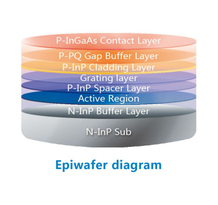
The n-type InP substrate provides excellent lattice matching for epitaxial layers, such as
InGaAsP, which are used to form the active region, cladding layers,
and the DFB laser's integrated grating structure. This grating
allows for precise feedback and wavelength control, making it ideal
for long-distance communication and Wavelength Division
Multiplexing (WDM) systems.
Key applications of DFB epiwafers on N-InP substrates include
high-speed optical transceivers, data center interconnects,
environmental gas sensing, and medical imaging through Optical
Coherence Tomography (OCT). The wafer's performance
characteristics, such as high-speed modulation, wavelength
stability, and narrow spectral linewidth, make it indispensable for
modern communication and sensing technologies.
DFB wafer N-InP substrate epiwafer's properties
Substrate Material: N-Type Indium Phosphide (N-InP)
- Lattice Matching: The N-InP substrate provides excellent lattice matching with
epitaxial layers, such as InGaAsP or InAlGaAs, reducing defects and
strain, which is critical for reliable, high-performance laser
operation.
- High Electron Mobility: InP has high electron mobility, enabling efficient carrier
transport, which is essential for high-speed DFB lasers.
- Direct Bandgap: InP has a direct bandgap of 1.344 eV, allowing for efficient
light emission in the infrared spectrum, specifically in the 1.3 µm
and 1.55 µm wavelength ranges.
Active Region and Epitaxial Layers
- InGaAsP/InAlGaAs Active Layer: The active region, typically made of InGaAsP, is where
electron-hole recombination occurs, generating photons. This region
is carefully designed to emit light in specific wavelength ranges
(1.3 µm or 1.55 µm) for optical communication.
- Cladding Layers: Surround the active region, providing optical confinement,
ensuring that light remains within the active region for efficient
lasing.
- Grating Layer: The DFB structure includes a built-in grating that provides
feedback for single-mode operation and precise wavelength control.
Operating Wavelength
Wavelength Stability
- Integrated Grating: The grating in the DFB structure ensures stable wavelength
output, making the laser highly reliable for long-distance
communication and WDM systems.
- Temperature Stability: DFB epiwafers on N-InP substrates offer excellent temperature
stability, ensuring consistent performance across a wide
temperature range.
Low Threshold Current
- The optimized structure of the DFB laser on an N-InP substrate
leads to low threshold currents, meaning less power is required to
initiate lasing, making these wafers highly energy-efficient.
High-Speed Modulation Capability
- Due to the high electron mobility and efficient carrier injection
in InP, DFB lasers on N-InP substrates are capable of high-speed
modulation, making them ideal for use in high-speed optical
transceivers and data center interconnects.
DFB wafer N-InP substrate epiwafer's PL mapping test(ZMSH DFB
inp epiwafer.pdf)

DFB wafer N-InP substrate epiwafer's XRD & ECV test result

DFB wafer N-InP substrate epiwafer's application
DFB (Distributed Feedback) wafers on n-type Indium Phosphide
(N-InP) substrates are crucial in various high-performance
optoelectronic applications, especially where single-mode,
narrow-linewidth light emission is required. Below are the primary
applications:
Optical Communication
- Long-Distance Fiber Optic Networks: DFB lasers on N-InP substrates
are widely used in long-distance optical communication systems.
Their single-mode output at wavelengths like 1.3 µm and 1.55 µm is
optimal for minimizing signal loss in optical fibers, making them
ideal for high-speed data transmission.
- WDM (Wavelength Division Multiplexing) Systems: In dense WDM
systems, DFB lasers are used to generate precise wavelengths for
different channels. Their narrow linewidth and wavelength stability
are essential for maximizing the number of channels in the optical
spectrum.
Data Center Interconnects
- High-Speed Data Transmission: DFB lasers are employed in optical
transceivers used for short- to medium-distance high-speed data
transmission within data centers. Their high-frequency modulation
capability and low power consumption are critical for
energy-efficient operations.
Environmental Gas Sensing
- Gas Detection: DFB lasers are used in environmental gas sensors to
detect specific gases, such as CO2 and CH4. By tuning the laser to
the absorption wavelength of these gases, highly sensitive
measurements can be made for industrial and environmental
monitoring applications.
- Laser Absorption Spectroscopy: DFB lasers provide narrow linewidth
and stable output, making them ideal for precise gas sensing and
spectroscopy applications.
Medical Diagnostics (Optical Coherence Tomography - OCT)
- Ophthalmology and Dermatology: DFB lasers are used in Optical
Coherence Tomography (OCT) systems, which are widely used for
high-resolution imaging of biological tissues. The narrow spectral
linewidth and stable wavelength output help generate clear and
detailed images, essential for non-invasive diagnostics in
ophthalmology and dermatology.
LIDAR (Light Detection and Ranging) Systems
- Autonomous Vehicles and 3D Mapping: DFB lasers are used in LIDAR
systems for measuring distances and mapping environments. Their
narrow linewidth and stable performance allow for accurate distance
measurements and object detection in autonomous driving, drones,
and 3D mapping systems.
Satellite and Space Communication
- High-Frequency Communication: DFB lasers are employed in satellite
communication systems to transmit high-frequency, long-distance
data signals. Their wavelength stability and low power consumption
are vital for reliable space communication, where temperature and
environmental conditions can vary.
Photonic Integrated Circuits (PICs)
- Integrated Optoelectronics: DFB epiwafers are used in photonic
integrated circuits (PICs), which combine multiple optical
components, such as lasers, modulators, and detectors, on a single
chip. These circuits are essential for applications in high-speed
data communication and signal processing.
Military and Aerospace
- Secure Communication and Targeting: DFB lasers are used in military
applications for secure, high-frequency communication. Their narrow
linewidth and wavelength stability are crucial for minimizing
signal interference in complex communication environments.
- Precision Targeting: In aerospace and defense, DFB lasers are
employed in targeting and guidance systems that require precise
wavelength control and stability.
Precision Spectroscopy
- Scientific Research: DFB lasers are used in precision spectroscopy
for detailed analysis of materials and chemical compositions. Their
narrow linewidth and tunable wavelength make them ideal for
accurate measurements in scientific research and industrial
applications.
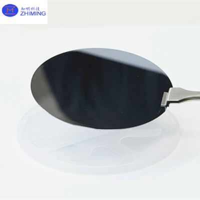
DFB wafer N-InP substrate epiwafer's real photos


Key words:DFB wafe,r N-InP substrate epiwafer,active layer
InGaAlAs/InGaAsP


