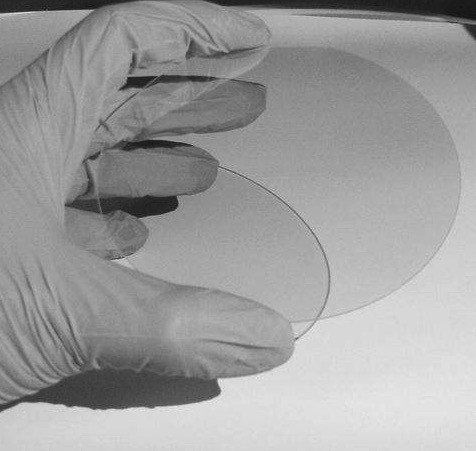
- use GaN on Si compound wafers to manufacture
- support customized ones with design artwork
- high-quality, suitable for high-performance applications
- high hardness and high efficiency, with high power density
- widely used in power electricity, RF devices, 5G and beyond, etc.
More about GaN on Si wafer
GaN-on-Si is a semiconductor material that combines the advantages
of gallium nitride (GaN) and silicon (Si).
GaN has the characteristics of wide bandgap, high electron mobility
and high-temperature resistance, which makes it have significant
advantage in high-frequency and high-power applications.
However, traditional GaN devices are usually based on expensive
substrate materials such as sapphire or silicon carbide.
In contrast, GaN-on-Si uses lower-cost and larger silicon wafers as
substrates, greatly reducing production costs and improving
compatibility with existing silicon-based processes.
This material is widely used in power electronics, RF devices and
optoelectronics.
For example, GaN-on-Si devices have shown excellent performance in
power management, wireless communications and solid-state lighting.
In addition, with the advancement of manufacturing technology,
GaN-on-Si is expected to replace traditional silicon-based devices
in a wider range of applications, promoting the further
miniaturization and efficiency of electronic devices.
Further details of GaN on Si wafer
| Parameter Category | parameter | Value/Range | Remark |
| Material properties | GaN Bandgap Width | 3.4 eV | Wide bandgap semiconductor, suitable for high temperature, high
voltage and high frequency applications |
| Silicon (Si) bandgap width | 1.12 eV | Silicon as substrate material provides better cost-effectiveness |
| Thermal conductivity | 130-170 W/m·K | The thermal conductivity of the GaN layer and the silicon substrate
is about 149 W/m·K |
| Electron mobility | 1000-2000 cm²/V·s | The electron mobility of the GaN layer is higher than that of
silicon |
| Dielectric constant | 9.5 (GaN), 11.9 (Si) | Dielectric Constants of GaN and Silicon |
| Coefficient of thermal expansion | 5.6 ppm/°C (GaN), 2.6 ppm/°C (Si) | The thermal expansion coefficients of GaN and silicon do not match,
which can cause stress |
| Lattice constant | 3.189 Å (GaN), 5.431 Å (Si) | The lattice constants of GaN and Si are not matched, which may lead
to dislocations |
| Dislocation density | 10⁸-10⁹ cm⁻² | Typical dislocation density of a GaN layer, depending on the
epitaxial growth process |
| Mechanical hardness | 9 Mohs | Gallium nitride's mechanical hardness provides wear resistance and
durability |
| Wafer specifications | Wafer diameter | 2 inches, 4 inches, 6 inches, 8 inches | Common GaN-on-Si wafer sizes |
| GaN layer thickness | 1-10 µm | Depends on specific application requirements |
| Substrate thickness | 500-725 µm | Typical thickness of silicon substrate, supporting mechanical
strength |
| Surface roughness | < 1 nm RMS | The roughness of the surface after polishing ensures high-quality
epitaxial growth |
| Step height | < 2 nm | The step height of the GaN layer affects device performance |
| Warpage | < 50 µm | The warpage of the wafer affects the compatibility of the
manufacturing process |
| Electrical properties | Electron concentration | 10¹⁶-10¹⁹ cm⁻³ | n-type or p-type doping concentration of GaN layer |
| Resistivity | 10⁻³-10⁻² Ω·cm | Typical resistivity of GaN layers |
| Breakdown electric field | 3 MV/cm | The high breakdown electric field strength of the GaN layer is
suitable for high voltage devices |
| Optical performance | Emission wavelength | 365-405 nm (UV/blue light) | The emission wavelength of GaN materials, used in optoelectronic
devices such as LEDs and lasers |
| Absorption coefficient | ~10⁴ cm⁻¹ | Absorption coefficient of GaN material in the visible light range |
| Thermal properties | Thermal conductivity | 130-170 W/m·K | The thermal conductivity of the GaN layer and the silicon substrate
is about 149 W/m·K |
| Coefficient of thermal expansion | 5.6 ppm/°C (GaN), 2.6 ppm/°C (Si) | The thermal expansion coefficients of GaN and silicon do not match,
which can cause stress |
| Chemical properties | Chemical stability | high | Gallium nitride has good corrosion resistance and is suitable for
harsh environments |
| Surface treatment | Dust-free and pollution-free | Cleanliness requirements for GaN wafer surface |
| Mechanical properties | Mechanical hardness | 9 Mohs | Gallium nitride's mechanical hardness provides wear resistance and
durability |
| Young's modulus | 350 GPa (GaN), 130 GPa (Si) | Young's modulus of GaN and silicon, affecting the mechanical
properties of the device |
| Production parameters | Epitaxial growth method | MOCVD, HVPE, MBE | Common methods for epitaxial growth of GaN layers |
| Yield | Depends on process control and wafer size | Yield rate is affected by factors such as dislocation density and
warpage |
| Growth temperature | 1000-1200°C | Typical temperatures for epitaxial growth of GaN layers |
| Cooling rate | Controlled cooling | To prevent thermal stress and warping, the cooling rate is usually
controlled |
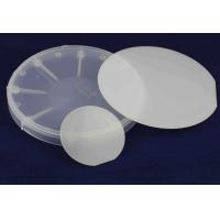
Samples of GaN on Si wafer

*Meanwhile, if you have any further requirements, please feel free
to contact us to customize one.
About us and the packaging box
About us
Our enterprise, ZMSH, specialises in the research, production,
processing, and sales of Semiconductor substrates and optical
crystal materials.
We have an experienced engineering team, management expertise,
precision processing equipment, and testing instruments, providing
us with extremely strong capabilities in processing non-standard
products.
We can research, develop, and design various new products according
to customer needs.
The company will adhere to the principle of "customer-centred,
quality-based" and strive to become a top-tier high-tech enterprise
in the field of optoelectronic materials.
About packaging box
Devoting to assisting our customers, we use wafer foam plastic to
package.
Here are some pictures of these.


