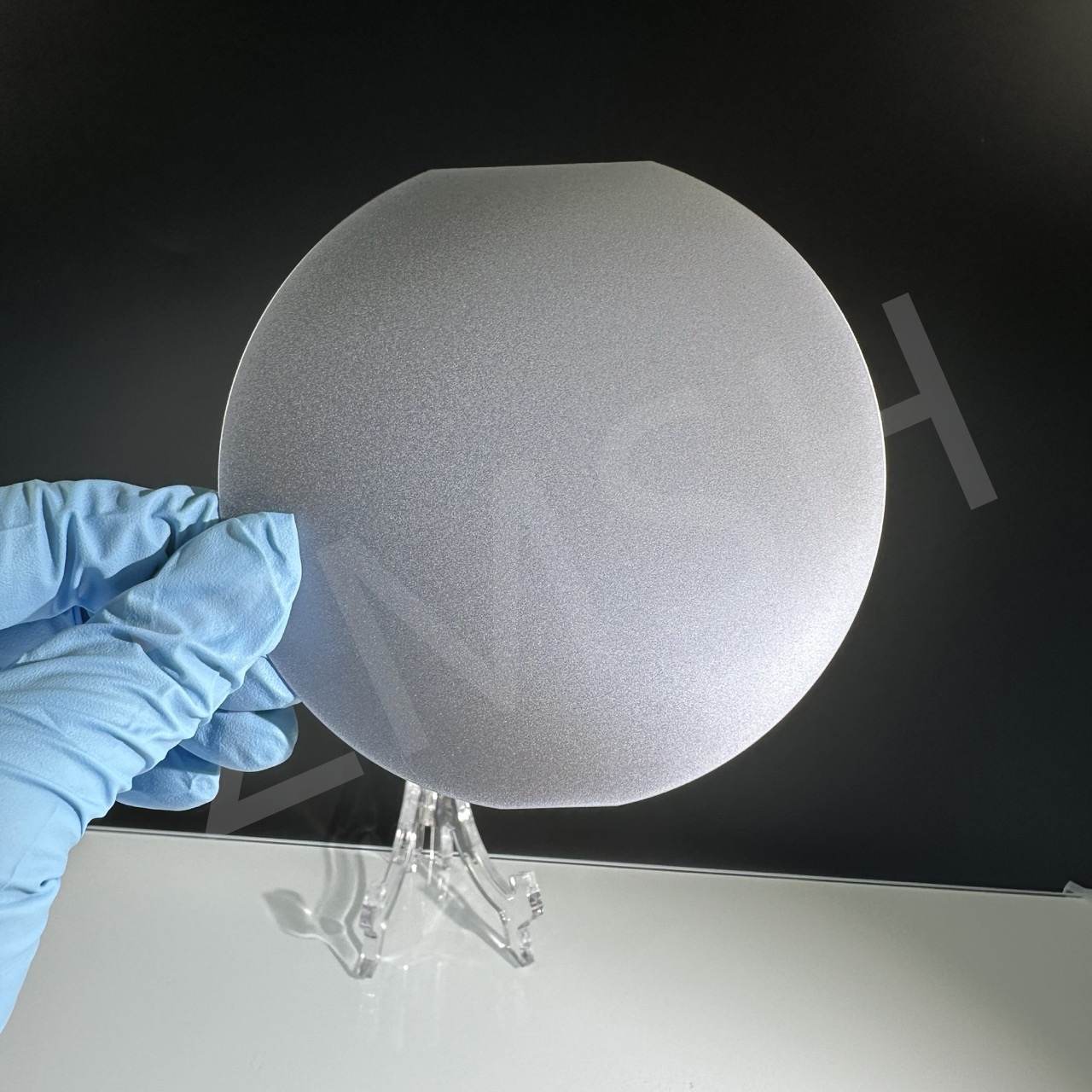
Semi-insulating SiC on Si Compound Wafer , Si wafer, Silicon Wafer,
Compound Wafer, SiC on Si Compound Substrate, Silicon Carbide
Substrate, P Grade, D Grade, 4inch, 6inch, 4H-SEMI
About Compound wafer
- use SiC on Si compound wafer to manufacture
- support customized ones with design artwork
- high-quality, suitable for high-performance applications
- high hardness and durability, high thermal conductivity
- widely used in high-voltage and high-frequency devices, RF devices,
etc.
More of Compound wafer
Semi-insulating SiC on Si Compound Wafer is a high-performance
advanced semiconductor material.
It has the advantages of both silicon substrate and semi-insulating
silicon carbide substrate.
It has excellent thermal conductivity and outstanding high
mechanical strength.
It can significantly reduce low leakage current under high
temperature and high-frequency conditions and effectively improve
device performance.
It is an excellent semiconductor material.
It is usually used in power electronics, radio frequency, and
optoelectronic devices, especially in high-demand applications
requiring excellent heat dissipation and electrical stability.
Although its production cost is relatively high compared to silicon
wafers and silicon carbide wafers, it has attracted more and more
attention and favour in high-performance technology due to its
advantages in improving device efficiency and stability
reliability.
Therefore, semi-insulating SiC on Si composite wafers has broad
development prospects in future high-end technology applications.
Details of Compound wafer
| Item | Specification |
| Diameter | 150 ± 0.2 mm |
| SiC Polytype | 4H |
| SiC Resistivity | ≥1E8 Ω·cm |
| Transfer SiC layer Thickness | ≥0.1 μm |
| Void | ≤5 ea/wafer (2 mm > D > 0.5 mm) |
| Front roughness | Ra ≤ 0.2 nm (5 μm × 5 μm) |
| Si Orientation | <111>/<100>/<110> |
| Si Type | P/N |
| Flat/Notch | Flat/Notch |
| Edge Chip, Scratch, Crack (visual inspection) | None |
| TTV | ≤5 μm |
| Thickness | 500/625/675 ± 25 μm |
Other pictures of Compound wafer
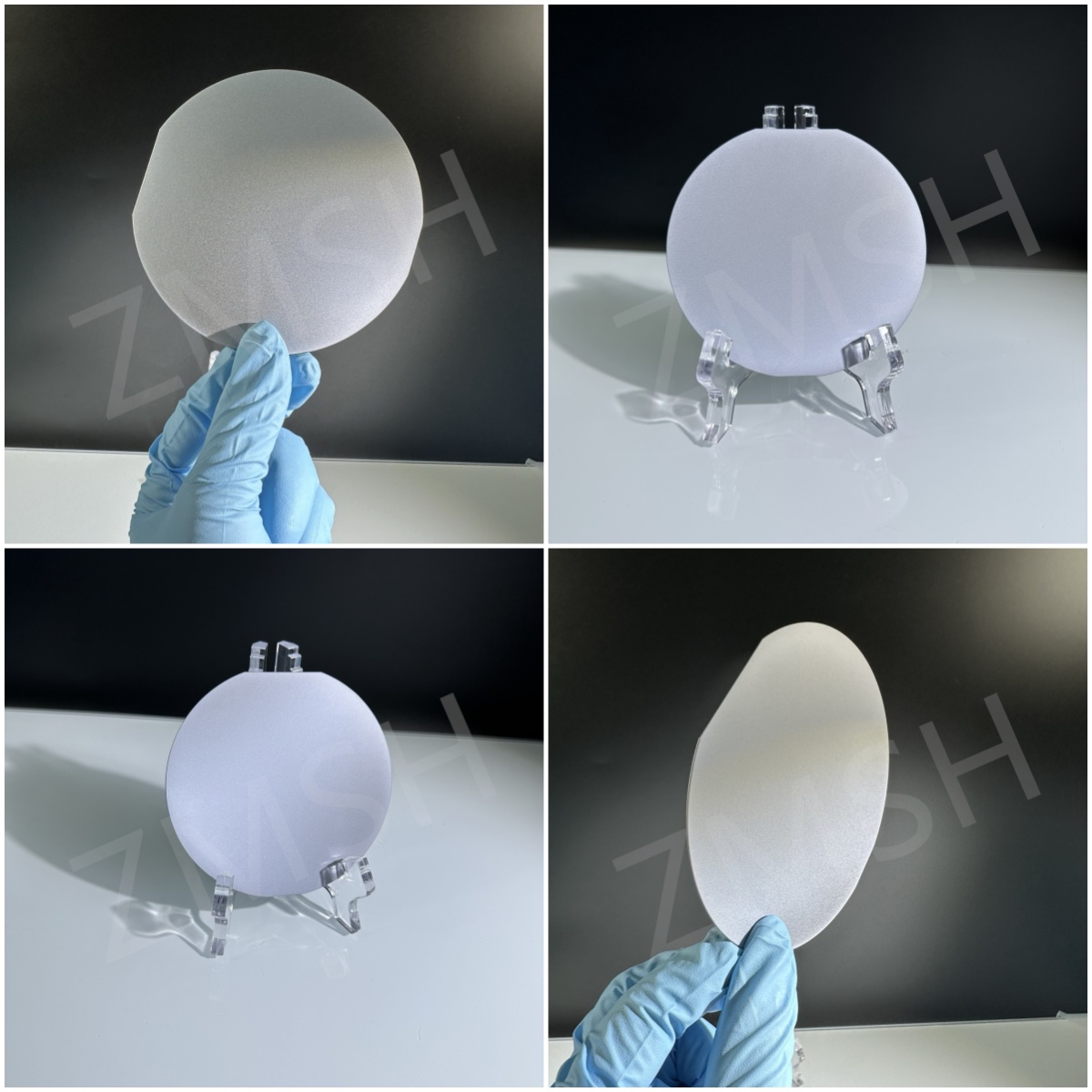

*Please feel free to contact us if you have customized demands.
About us
Our enterprise, ZMSH, specialises in the research, production,
processing, and sales of Semiconductor substrates and optical
crystal materials.
We have an experienced engineering team, management expertise,
precision processing equipment, and testing instruments, providing
us with extremely strong capabilities in processing non-standard
products.
We can research, develop, and design various new products according
to customer needs.
The company will adhere to the principle of "customer-centred,
quality-based" and strive to become a top-tier high-tech enterprise
in the field of optoelectronic materials.
Similar product recommendations
1.
4H-SEMI Silicon Carbide SiC
Substrate 2 Inch Thickness 350um 500um P Grade D Grade SiC
Wafer

2. 2"
3" FZ SiO2 Single Crystal IC Chips 100um 200um Dry Wet Oxidation
Layer 100nm 300nm

FAQ
1. Q: What is the common surface orientation of SiC on Si wafers?
A: The common orientation is (111) for SiC, aligned with the
silicon substrate.
2. Q: Are there specific annealing requirements for SiC on Si
wafers?
A: Yes, high-temperature annealing is often required to improve
material properties and reduce defects.


