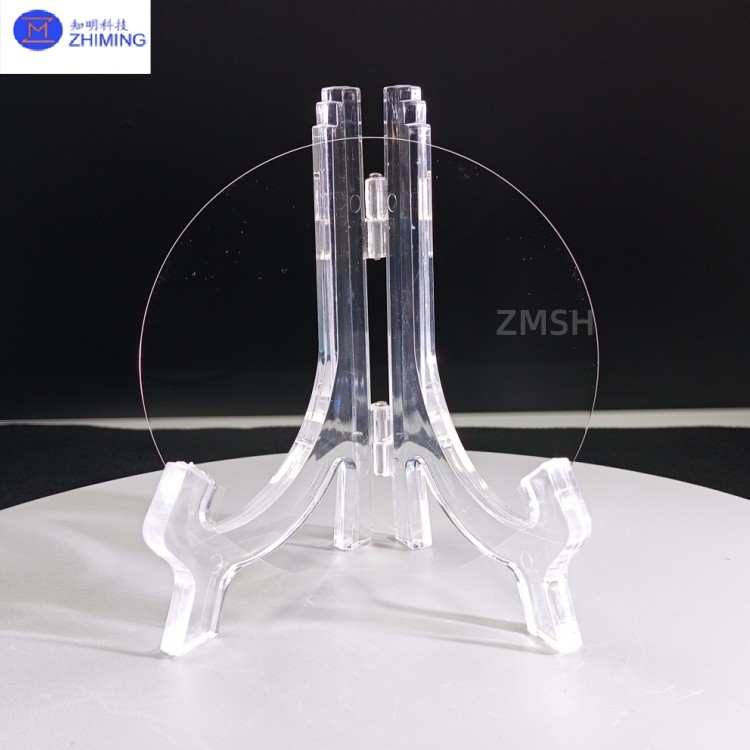
Sapphire Wafer – Off C-axis toward M-plane 8° , Al₂O₃, Diameter 2"/3"/4"/6"/8", Custom Thickness
This high-precision sapphire wafer features a 8° off from C-axis toward M plane orientation and 99.999% (5N) purity, optimized for superior epitaxial growth in advanced
optoelectronic and semiconductor applications. Available in standard diameters (2" to 8") with customizable thicknesses, it provides exceptional
crystallographic uniformity, ultra-low defect density, and
outstanding thermal/chemical stability. The controlled 1° off-cut
angle enhances GaN and AlN epitaxy by reducing step-bunching
defects, making it ideal for high-performance LEDs, laser diodes,
power electronics, and RF devices.
Key Features of Sapphire Wafer
Precision Off-Cut Orientation
8° off from C-axis toward M plane, engineered to improve epitaxial film uniformity and minimize
defects in GaN-based devices.
Ultra-High Purity (5N Al₂O₃)
99.999% purity with trace impurities (Fe, Ti, Si) <5 ppm, ensuring optimal
electrical and optical performance.
Diameters: 2", 3", 4", 6", 8" (±0.1 mm tolerance).
Thickness: 100 µm to 1,500 µm (±5 µm tolerance), tailored for

specific applications.
Epi-ready polish: Ra <0.5 nm (front side) for defect-free thin-film deposition.
Thermal stability: Melting point ~2,050°C, suitable for
high-temperature processes (MOCVD, MBE).
Optical transparency: >85% transmission (UV to mid-IR: 250 nm–5,000 nm).
Mechanical robustness: 9 Mohs hardness, resistant to chemical etching and abrasion.
Applications of Sapphire Wafer
Optoelectronics
GaN-based LEDs/Laser Diodes: Blue/UV LEDs, micro-LEDs, and VCSELs.
High-power laser windows: CO₂ and excimer laser components.
Power & RF Electronics
HEMTs (High-Electron-Mobility Transistors): 5G/6G power amplifiers and radar systems.
Schottky diodes and MOSFETs: High-voltage devices for electric vehicles.
Industrial & Defense
IR windows and missile domes: High transparency in harsh environments.
Sapphire sensors: Corrosion-resistant covers for industrial monitoring.
Quantum & Research Technologies
Substrates for superconducting qubits (quantum computing).
SPDC (Spontaneous Parametric Down-Conversion) crystals for quantum optics.
Semiconductor & MEMS
SOI (Silicon-on-Insulator) wafers for advanced ICs.
MEMS pressure sensors requiring chemical inertness.


Specifications
Parameter | Value |
|---|
| Diameter | 2", 3", 4", 6", 8" (±0.1 mm) |
| Thickness | Custom (100–1,500 µm ±5 µm) |
| Orientation | off C-axis toward M plane 8° |
| Purity | 99.999% (5N Al₂O₃) |
| Surface Roughness (Ra) | <0.5 nm (epi-ready) |
| Dislocation Density | <500 cm⁻² |
| TTV (Total Thickness Variation) | <10 µm |
| Bow/Warp | <15 µm |
| Optical Transparency | 250–5,000 nm (>85%) |
Q&A
Q1: Can I request a different off-cut angle (e.g., 0.5° or 2°)?
A2: Yes. Custom off-cut angles are available with ±0.1° tolerance.
Q2: What’s the maximum thickness available?
A6: Up to 1,500 µm (1.5 mm) for mechanical stability in high-stress applications.
Q3: How should wafers be stored to prevent contamination?
A10: Store in cleanroom-compliant cassettes or nitrogen cabinets (20–25°C, humidity <40%).


