Wafer Bonding Equipment Room Temperature Bondin Hydrophilic Bonding
Si-SiC Si-Si Bonding 2 -12 inch
Wafer Bonding System Overview
Wafer Bonding Equipment is a high-end bonding equipment
specifically designed for silicon carbide (SiC) power device
manufacturing, supporting 2 to 12-inch wafer specifications. Wafer
Bonding Equipment incorporates advanced room-temperature direct
bonding and surface-activated bonding technologies, with special
optimization for SiC-SiC and SiC-Si heterogeneous bonding
processes. Featuring an integrated high-precision optical alignment
system (≤±2 μm) and closed-loop temperature/pressure control, it
ensures the high bonding strength (≥2 J/m²) and superior interface
uniformity required for power semiconductor device fabrication.
Wafer Bonding System Technical Specifications
Core Functional Parameters:
| Bonding Processes: | Supports direct bonding and plasma-activated bonding |
| Wafer Compatibility: | Full-range 2"-12" wafer handling |
| Material Combinations: | Si-SiC/SiC-SiC heterostructure bonding |
| Alignment System: | Ultra-high precision optical alignment (≤±0.5 μm) |
| Pressure Control: | Precision adjustable 0-10 MPa |
| Temperature Range: | RT-500°C (optional preheat/annealing module) |
| Vacuum Level: | Ultra-high vacuum environment (≤5×10⁻⁶ Torr) |
Intelligent Control System:
· Industrial-grade touch HMI
· ≥50 stored process recipes
· Real-time pressure-temperature closed-loop feedback
Safety Protection System:
· Triple interlock protection (pressure/temperature/vacuum)
· Emergency braking system
· Class 100 cleanroom compatibility
Extended Functions:
· Optional robotic wafer handling
· SECS/GEM communication protocol support
· Integrated inline inspection module
Wafer Bonding Equipment is specifically designed for R&D and
mass production of third-generation semiconductors. Wafer Bonding
Equipment modular architecture enables high-reliability bonding for
SiC-based power devices. The innovative plasma pretreatment
technology significantly enhances interfacial bonding strength (≥5
J/m²), while the ultra-high vacuum environment ensures
contaminant-free bonding interfaces. The intelligent
temperature-pressure control system, combined with submicron
alignment accuracy, provides wafer-level bonding solutions for
HEMT, SBD and other devices.
Photo
Compatible Materials

Applications
· MEMS Device Packaging: Wafer Bonding Equipment is suitable for
hermetic sealing of microelectromechanical systems (MEMS) such as
accelerometers and gyroscopes.
· CIS Image Sensors: Wafer Bonding Equipment enables
low-temperature bonding between CMOS wafers and optical glass
substrates.
· 3D IC Integration: Wafer Bonding Equipment supports
room-temperature stacking bonding for through-silicon via (TSV)
wafers.
· Compound Semiconductor Devices: Wafer Bonding Equipment
facilitates epitaxial layer transfer for GaN/SiC power devices.
· Biochip Fabrication: Wafer Bonding Equipment provides
low-temperature packaging solutions for microfluidic chips.
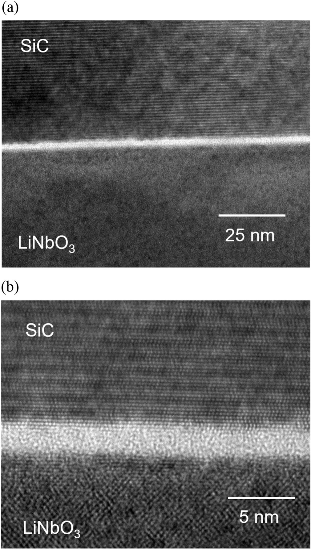
Machining effect——Bonding of LiNbO 3 wafer and SiC wafer
( (a) Photograph of LiNbO3/SiC wafers bonded at room temperature.
(b) Photograph of diced 1 × 1 mm chips. )

( (a) Cross-sectional TEM image of the LiNbO₃/SiC bonding interface
(b) Magnified view of (a) )