Microjet laser technology equipment wafer slice metal silicon
carbide material
Microjet Laser systems enable ultra-precision machining of
semiconductor materials by coupling high-energy pulsed lasers to
micron-scale liquid jets (usually deionized water or inert
liquids), using the guiding and cooling effects of the liquid jets.
With high precision, low damage and high cleanliness, microjet
laser technology is replacing traditional machining and dry laser
processes in the semiconductor field, especially in
third-generation semiconductors (SiC/GaN), 3D packaging and
ultra-thin wafer processing.
Microjet laser processing

Technical specifications
| Countertop volume | 300*300*150 | 400*400*200 |
| Linear axis XY | Linear motor. Linear motor | Linear motor. Linear motor |
| Linear axis Z | 150 | 200 |
| Positioning accuracy μm | +/-5 | +/-5 |
| Repeated positioning accuracy μm | +/-2 | +/-2 |
| Acceleration G | 1 | 0.29 |
| Numerical control | 3 axis /3+1 axis /3+2 axis | 3 axis /3+1 axis /3+2 axis |
| Numerical control type | DPSS Nd:YAG | DPSS Nd:YAG |
| Wavelength nm | 532/1064 | 532/1064 |
| Rated power W | 50/100/200 | 50/100/200 |
| Water jet | 40-100 | 40-100 |
| Nozzle pressure bar | 50-100 | 50-600 |
| Dimensions (machine tool) (width * length * height) mm | 1445*1944*2260 | 1700*1500*2120 |
| Size (control cabinet) (W * L * H) | 700*2500*1600 | 700*2500*1600 |
| Weight (equipment) T | 2.5 | 3 |
| Weight (control cabinet) KG | 800 | 800 |
Processing capability | Surface roughness Ra≤1.6um Opening speed ≥1.25mm/s Circumference cutting ≥6mm/s Linear cutting speed ≥50mm/s | Surface roughness Ra≤1.2um Opening speed ≥1.25mm/s Circumference cutting ≥6mm/s Linear cutting speed ≥50mm/s |
For gallium nitride crystal, ultra-wide band gap semiconductor
materials (diamond/Gallium oxide), aerospace special materials,
LTCC carbon ceramic substrate, photovoltaic, scintillator crystal
and other materials processing. Note: Processing capacity varies depending on material
characteristics
|

Microjet laser equipment technical advantages
1. Small loss of processing materials and processing equipment
2. Greatly reduce grinding links
3. Low labor cost of automated processing
4. High quality machining wall and cutting edge
5. Clean processing without environmental pollution
6. High processing efficiency
7. High processing yield
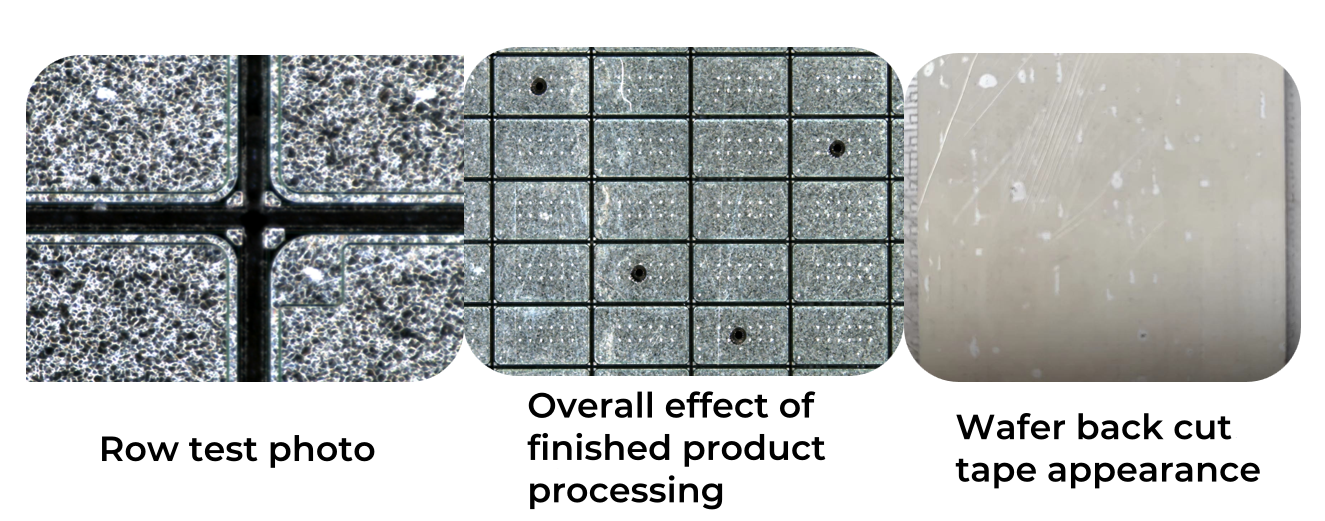
Microfluidic laser silicon wafer scribing
Test with the debugging processing parameters, and the cutting
effect is shown in the figure below. The cutting width of 40μm
nozzle is 35um; After the cutting is completed, the wafer is
completely scratched, and the back of the cutting tape (UV film) is
basically intact and not scratched through. There is no cracking
and crack on the edge of the crossing, which meets the processing
requirements.
Q&A


