4inch dia100m 4H-N type Production grade DUMMY grade SiC
substrates,Silicon Carbide substrates for semiconductor device,
customized thickness 4inch 4H-N silicon carbide crystal sic wafers for 4inch seed crystal grade;
Silicon Carbide SiC crystal substrate wafer carborundum
SILICON CARBIDE MATERIAL PROPERTIES
| Product Name: | Silicon carbide (SiC) crystal substrate |
| Product Description: | 2-6inch |
| Technical parameters: | | Cell structure | Hexagonal | | Lattice constant | a = 3.08 Å c = 15.08 Å | | Priorities | ABCACB (6H) | | Growth method | MOCVD | | Direction | Growth axis or Partial (0001) 3.5 ° | | Polishing | Si surface polishing | | Bandgap | 2.93 eV (indirect) | | Conductivity type | N or seimi ,high purity | | Resistivity | 0.076 ohm-cm | | Permittivity | e (11) = e (22) = 9.66 e (33) = 10.33 | | Thermal conductivity @ 300K | 5 W / cm. K | | Hardness | 9.2 Mohs |
|
| Specifications: | 6H N-type 4H N-type semi-insulating dia2 "x0.33mm, dia2"
x0.43mm,dia2''x1mmt, 10x10mm, 10x5mm Single throw or double throw,
Ra <10A |
| Standard Packaging: | 1000 clean room, 100 clean bag or single box packaging |
Application of silicon carbide in power device industry
Compared with silicon (Si) devices, silicon carbide (SiC) power
devices can effectively achieve high efficiency, miniaturization
and light weight of power electronic systems. The energy loss of
silicon carbide power devices is only 50% of that of Si devices,
the heat generation is only 50% of that of silicon devices, and it
has a higher current density. At the same power level, the volume
of silicon carbide power modules is significantly smaller than that
of silicon power modules. Taking the intelligent power module IPM
as an example, using silicon carbide power devices, the module
volume can be reduced to 1/3 to 2/3 of silicon power modules.
There are 3 types of silicon carbide power diodes: Schottky diodes
(SBD), PIN diodes and junction barrier control Schottky diodes
(JBS). Due to the Schottky barrier, SBD has a lower junction
barrier height, so SBD has the advantage of low forward voltage.
The emergence of silicon carbide SBD increased the application
range of SBD from 250V to 1200V. At the same time, its high
temperature characteristics are good, from room temperature to
175°C limited by the shell, the reverse leakage current hardly
increases. In the application field of rectifiers above 3kV,
silicon carbide PiN and silicon carbide JBS diodes have attracted
attention due to their higher breakdown voltage, faster switching
speed, smaller volume and lighter weight than silicon rectifiers.
Silicon carbide power MOSFET devices have ideal gate resistance,
high-speed switching performance, low on-resistance and high
stability. It is the preferred device in the field of power devices
below 300V. It is reported that a silicon carbide MOSFET with a
blocking voltage of 10kV has been successfully developed.
Researchers believe that silicon carbide MOSFET will occupy an
advantageous position in the field of 3kV to 5kV.
Silicon carbide insulated gate bipolar transistors (SiC BJT, SiC
IGBT) and silicon carbide thyristors (SiC Thyristor), silicon
carbide P-type IGBT devices with a blocking voltage of 12kV have
good forward current capability. The on-resistance of silicon
carbide IGBT devices can be compared with unipolar silicon carbide
power devices. Compared with Si bipolar transistors, SiC bipolar
transistors have 20-50 times lower switching losses and lower
conduction voltage drop. Silicon carbide BJT is mainly divided into
epitaxial emitter and ion implanted emitter BJT, and the typical
current gain is between 10-50.
Performance Unit Silicon Si Silicon Carbide SiC Gallium Nitride GaN
Band gap eV 1.12 3.26 3.41
Breakdown electric field MV/cm 0.23 2.2 3.3
Electron mobility cm^2/Vs 1400 950 1500
Drift speed 10^7 cm/s 1 2.7 2.5
Thermal conductivity W/cmK 1.5 3.8 1.3
2. substrates size of standard
4 inch diameter Silicon Carbide (SiC) Substrate Specification |
| Grade | Zero MPD Grade | Production Grade | Research Grade | Dummy Grade |
| Diameter | 100.0 mm±0.5 mm |
| Thickness | 350 μm±25μm (200-2000um thickness also is ok) |
| Wafer Orientation | Off axis : 4.0° toward <1120> ±0.5° for 4H-N |
| Micropipe Density | ≤1 cm-2 | ≤5 cm-2 | ≤15 cm-2 | ≤50 cm-2 |
| Resistivity | 4H-N | 0.015~0.028 Ω•cm |
| 6H-N | 0.02~0.1 Ω•cm |
| 4/6H-SI | ≥1E5 Ω·cm |
| Primary Flat and length | {10-10}±5.0° ,32.5 mm±2.0 mm |
| Secondary Flat Length | 18.0mm±2.0 mm |
| Secondary Flat Orientation | Silicon face up: 90° CW. from Prime flat ±5.0° |
| Edge exclusion | 3 mm |
| TTV/Bow /Warp | ≤15μm /≤25μm /≤40μm |
| Roughness | Polish Ra≤1 nm ,CMP Ra≤0.5 nm |
| Cracks by high intensity light | None | 1 allowed, ≤2 mm | Cumulative length ≤ 10mm, single length≤2mm |
|
| Hex Plates by high intensity light | Cumulative area ≤1% | Cumulative area ≤1% | Cumulative area ≤3% |
| Polytype Areas by high intensity light | None | Cumulative area ≤2% | Cumulative area ≤5% |
| Scratches by high intensity light | 3 scratches to 1×wafer diameter cumulative length | 5 scratches to 1×wafer diameter cumulative length | 5 scratches to 1×wafer diameter cumulative length |
| edge chip | None | 3 allowed, ≤0.5 mm each | 5 allowed, ≤1 mm each |
| Contamination by high intensity light | None |
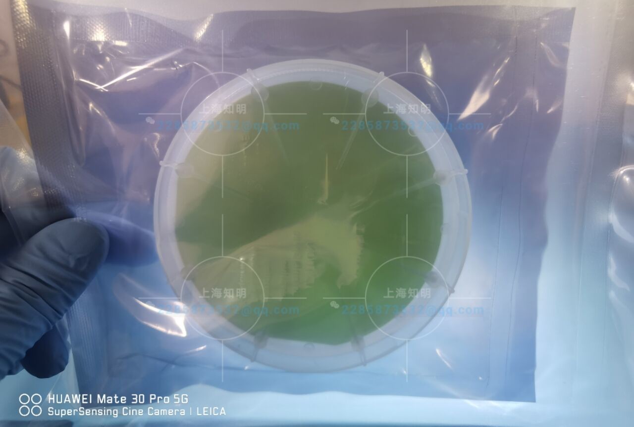
Sic wafer & ingots 2-6inch and other customized size also can be
provided.
3.Products detail display


Delivery & Package

FAQ
Q1. Is your company a factory or trade company?
We are the factory and we also can do export ourself.
Q2.Is you company only work with sic business?
yes; however we don‘t grow the sic crystal by self.
Q3. Could you supply sample?
Yes,we can supply sapphire sample according to customer's
requirement.
Q4. Do you have any stock of sic wafers ?
we usually keep some standard size sic wafers from 2-6inch wafers
in stock.
Q5.Where is your company located?
Our company located in shanghai ,China.
Q6. How long will take to get the products?
Generally it will take 3~4 weeks to process.It is depend on the
quantity and the size of the products.


