3inch VGF GaAs wafers Research test grade N-Type GaAs substrates 425um
2inch 3inch 4inch 6inch VGF method N-Type un-doped GaAs substrates 2degree off 675um SSP DSP GaAs wafers
------------------------------------------------------------------------------------------------------------------------------
GaAs wafer (Gallium Arsenide) is an advantageous alternative to silicon that has been evolving in the semiconductor industry. Less power consumption and more efficiency offered by this GaAs wafers are attracting the market players to adopt these wafers, thereby increasing the demand for GaAs wafer. Generally, this wafer is used to manufacture semiconductors, light emitting diodes, thermometers, electronic circuits, and barometers, besides finding application in the manufacturing of low melting alloys. As the semiconductor and electronic circuit industries continue to touch new peaks, the GaAs market is booming. Gallium arsenide of GaAs wafer has the power of generating laser light from electricity. Especially polycrystalline and single crystal are the two major type of GaAs wafers, which are utilized in the production of both the microelectronics and optoelectronics to create LD, LED, and microwave circuits. Therefore, the extensive range of GaAs applications, particularly in optoelectronics and microelectronics industry is creating a demand influx in the GaAs Wafer Market. Previously, the optoelectronic devices were mainly used on a broad range in short-range optical communications and computer peripherals. But now, they are in demand for some emerging applications such as LiDAR, augmented reality, and face recognition. LEC and VGF are two popular methods which are improving the production of GaAs wafer with high uniformity of electrical properties and excellent surface quality. Electron mobility, single junction band-gap, higher efficiency, heat and moisture resistance, and superior flexibility are the five distinct advantages of GaAs, which are improving the acceptance of GaAs wafers in the semiconductor industry.
Specification detail
| GaAs (Gallium Arsenide) for LED Applications |
| Item | Specifications | Remarks |
| Conduction Type | SC/n-type | |
| Growth Method | VGF | |
| Dopant | Silicon | |
| Wafer Diamter | 2, 3 & 4 inch | Ingot or as-cut available |
| Crystal Orientation | (100)2°/6°/15° off (110) | Other misorientation available |
| OF | EJ or US | |
| Carrier Concentration | (0.4~2.5)E18/cm3 | |
| Resistivity at RT | (1.5~9)E-3 Ohm.cm | |
| Mobility | 1500~3000 cm2/V.sec | |
| Etch Pit Density | <500/cm2 | |
| Laser Marking | upon request | |
| Surface Finish | P/E or P/P | |
| Thickness | 220~350um | |
| Epitaxy Ready | Yes | |
| Package | Single wafer container or cassette | |
| GaAs (Gallium Arsenide) ,Semi-insulating for Microelectronics Applications |
| Item | Specifications | Remarks |
| Conduction Type | Insulating | |
| Growth Method | VGF | |
| Dopant | Undoped | |
| Wafer Diamter | 2, 3, 4 & 6 inch | Ingot available |
| Crystal Orientation | (100)+/- 0.5° | |
| OF | EJ, US or notch | |
| Carrier Concentration | n/a | |
| Resistivity at RT | >1E7 Ohm.cm | |
| Mobility | >5000 cm2/V.sec | |
| Etch Pit Density | <8000 /cm2 | |
| Laser Marking | upon request | |
| Surface Finish | P/P | |
| Thickness | 350~675um | |
| Epitaxy Ready | Yes | |
| Package | Single wafer container or cassette | |
| No. | Item | Standard Specification |
| 1 | Size | | 2" | 3" | 4" | 6" |
| 2 | Diameter | mm | 50.8±0.2 | 76.2±0.2 | 100±0.2 | 150±0.5 |
| 3 | Growth Method | | VGF |
| 4 | Doped | | Un-doped, or Si-doped, or Zn-doped |
| 5 | Conductor Type | | N/A, or SC/N, or SC/P |
| 6 | Thickness | μm | (220-350)±20 or (350-675)±25 |
| 7 | Crystal Orientation | | <100>±0.5 or 2 off |
| OF/IF Orientation Option | | EJ, US or Notch |
| Orientation Flat (OF) | mm | 16±1 | 22±1 | 32±1 | - |
| Identification Flat (IF) | mm | 8±1 | 11±1 | 18±1 | - |
| 8 | Resistivity | (Not for
Mechanical
Grade) | Ω.cm | (1-30)´107, or (0.8-9)´10-3, or 1´10-2-10-3 |
| Mobility | cm2/v.s | ≥ 5,000, or 1,500-3,000 |
| Carrier Concentration | cm-3 | (0.3-1.0)x1018, or (0.4-4.0)x1018,
or As SEMI |
| 9 | TTV | μm | ≤10 |
| Bow | μm | ≤10 |
| Warp | μm | ≤10 |
| EPD | cm-2 | ≤ 8,000 or ≤ 5,000 |
| Front/Back Surface | | P/E, P/P |
| Edge Profile | | As SEMI |
| Particle Count | | <50 (size>0.3 μm,count/wafer),
or AS SEMI |
| 10 | Laser Mark | | Back side or upon request |
| 11 | Packaging | | Single wafer container or cassette |


ABOUT OUR ZMKJ
ZMKJ locates in the city of Shanghai, Which is the best city of China, and our factory is founded
in Wuxi city in 2014.We specialize in processing a varity of materials into wafers, substrates
and custiomized optical glass parts.components widely used in electronics, optics,
optoelectronics and many other fields. We also have been working closely with many domestic
and oversea universities, research institutions and companies, provide customized products
and services for their R&D projects.
It's our vision to maintaining a good relationship of cooperation with our all customers by our
good reputatiaons. so we also can provide some other materials substrates as like:
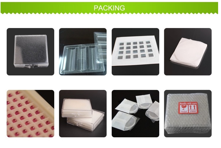
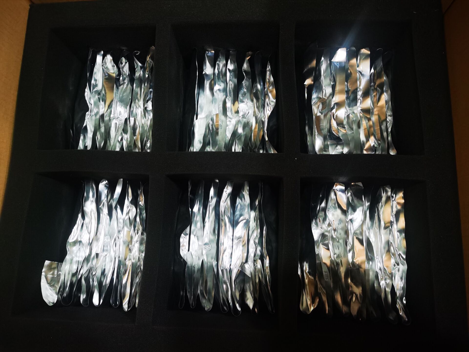
Packaging – Logistcs
Worldhawk concerns each details of the package , cleaning, anti-static , shock treatment .
According to the quantity and shape of the product , we will take a different packaging process!
FAQ –
Q: What you can supply logistics and cost?
(1) We accept DHL, Fedex, TNT, UPS, EMS, SF and by FOB
and pay condition of 50% deposit,50% before delivery.
Q: What's the delivery time?
For inventory: the delivery is 5 workdays after order.
For customized products: the delivery is 2 or 3 workweeks after order.
Q: What's the MOQ?
(1) For inventory, the MOQ is 5pcs.
(2) For customized products, the MOQ is 10pcs-30pcs.
Q: Do you have inspection report for material?
We can supply detail report for our products.