4inch 6inch 8inch 4H-N sic wafers dummy Prime Production grade for
SBD MOS Device, 8inch 6inch 4H-N Type Sic Substrate Wafer
Production Grade For Radio Frequency Devices
SiC feature
SiC (Silicon Carbide) is a compound material consists of silicon
(Si) and carbon (C), that has high hardness and heat resistance,
and it’s chemically stable.
As it has a wide bandgap, the application to the semiconductor
material is getting promoted.
With the high accuracy and high rigid grinding system of our edge
grinder, smooth finish can be achieved even with SiC wafer that is
difficult to cut material.
Comparison of third-generation semiconductor materials
SiC crystal is a third-generation semiconductor material, which has
great advantages in low-power, miniaturization, high-voltage and
high-frequency application scenarios. The third-generation
semiconductor materials are represented by silicon carbide and
gallium nitride. Compared with the previous two generations of
semiconductor materials, the biggest advantage is its wide
band-free width, which ensures that it can penetrate higher
electric field strength and is suitable for preparing high-voltage
and high-frequency power devices.
Classification
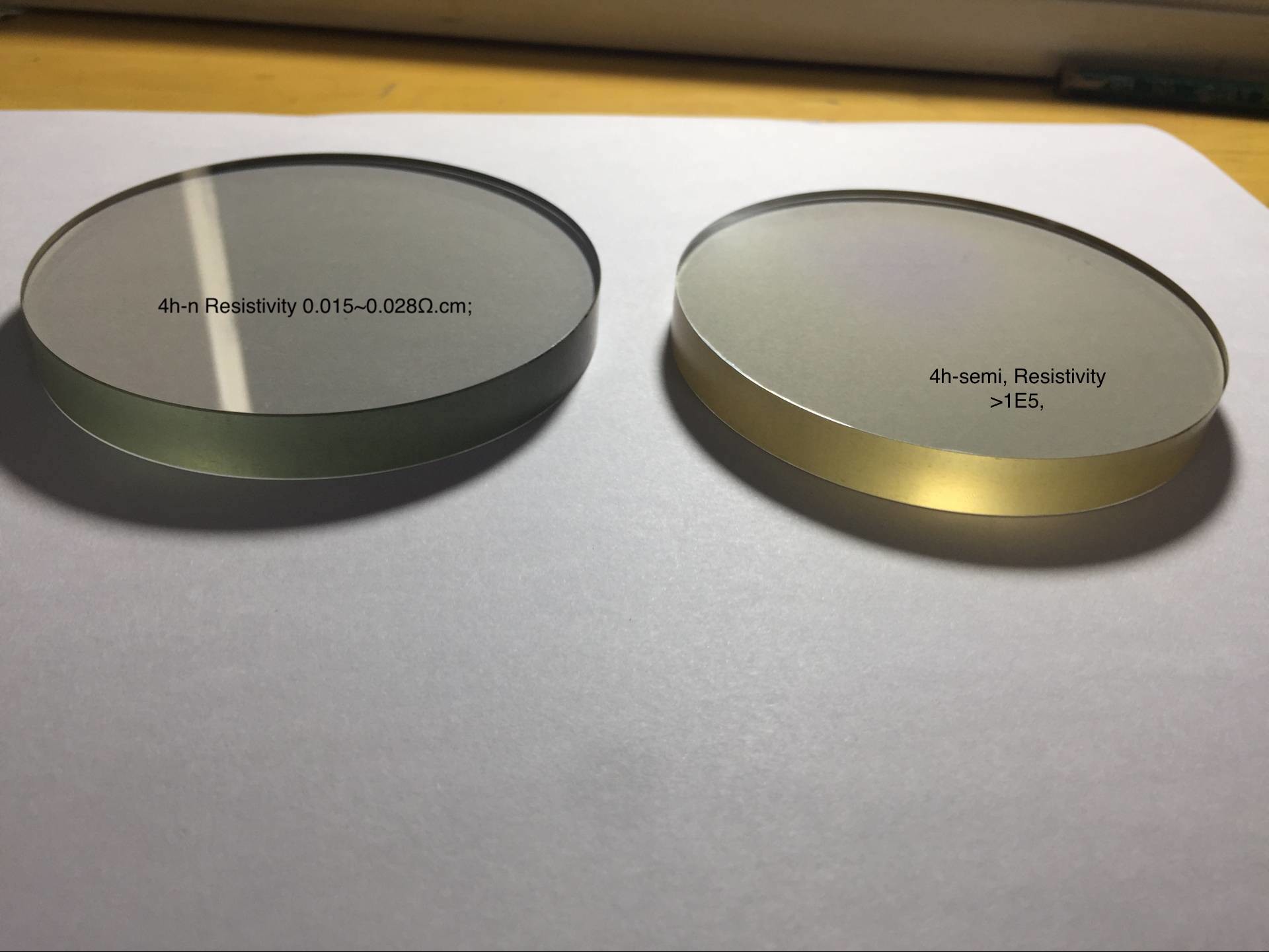
Silicon carbide SiC substrates can be divided into two categories:
semi-insulated (High Purity un-dopend and V-doped 4H-SEMI) silicon
carbide substrates with high resistivity (resistorivity ≥107Ω·cm),
and conductive silicon carbide substrates with low resistivity (the
resistivity range is 15-30mΩ·cm).
Application

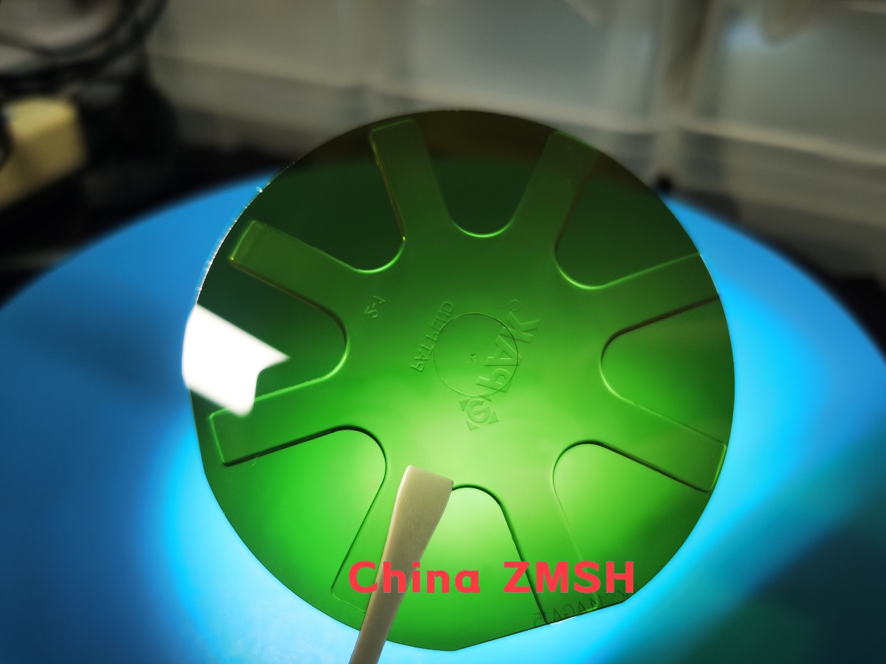
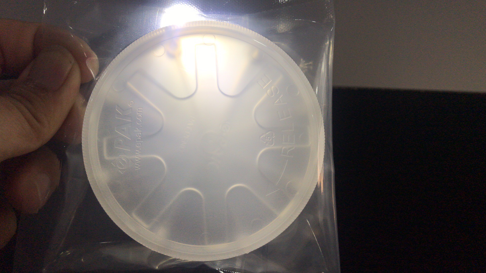
Specification for 8inch 4H-N sic wafers .(2inch,3inch 4inch ,8inch
sic wafer also is avaiable)
- Size: 8inch;
- Diameter: 200mm±0.2;
- Thickness: 500um±25;
- Surface Orientation: 4 toward [11-20]±0.5°;
- Notch orientation:[1-100]±1°;
- Notch depth: 1±0.25mm;
- Micropipe: <1cm2;
- Hex Plates: None Permitted;
- Resistivity: 0.015~0.028Ω;
- EPD:<8000cm2;
- TED:<6000cm2
- BPD:<2000cm2
- TSD:<1000cm2
- SF: area<1%
- TTV≤15um;
- Warp≤40um;
- Bow≤25um;
- Poly areas: ≤5%;
- Scratch: <5 and Cumulative Length< 1 Wafer Diameter;
- Chips/Indents: None permit D>0.5mm Width and Depth;
- Cracks: None;
- Stain: None
- Wafer edge: Chamfer;
- Surface finish: Double Side Polish, Si Face CMP;
- Packing: Multi-wafer Cassette Or Single Wafer Container;
The silicon carbide SiC industrial chain is divided into substrate
material preparation, epitaxial layer growth, device manufacturing
and downstream applications. Silicon carbide monocrystals are
usually prepared by physical vapor transmission (PVT method), and
then epitaxial sheets are generated by chemical vapor deposition
(CVD method) on the substrate, and the relevant devices are finally
made. In the industrial chain of SiC devices, due to the difficulty
of substrate manufacturing technology, the value of the industrial
chain is mainly concentrated in the upstream substrate link.
Related products

Why choose ZMSH company
- Complete production chain from cutting to final cleaning and
packing.
- Capability to reclaim wafers with diameters 4-inch—12-inch.
- 20 year experience of wafering and reclaiming of monocrystalline
electronic materials
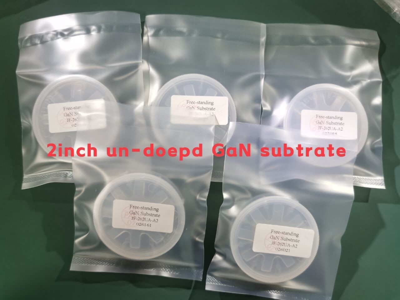
ZMSH Technology can provide customers with imported and domestic
high-quality conductive, 2-6inch semi-insulating and HPSI (High
Purity Semi-insulating) SiC substrates in batches; In addition, it
can provide customers with homogeneous and heterogeneous silicon
carbide epitaxial sheets, and can also be customized according to
the specific needs of customers, with no minimum order quantity.
Contact us
Monica Liu
Tel: +86-198-2279- 1220(whatsapp or skype is available )
Email:monica@zmsh-materials.com
Company: SHANGHAI FAMOUS TRADE CO.,LTD.
Factory: WUXI JINGJING TECHNOLOGY CO.,LTD.
Address: Room.5-616,No.851 Dianshanhu Road,Qingpu Area
Shanghai city, China /201799
We are focus on semiconductor
crystal(GaN;SiC;Sapphire;GaAs;InP;Silicon;MgO,LT/LN; etc.)


