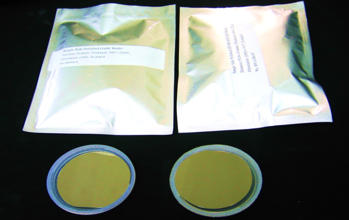
32inch InAs wafers N-type un-doped type GaAs wafers GaSb Wafers
Application
InAs single crystal can be used as substrate material to grow
InAsSb/InAsPSb, InNAsSb and other heterojunction materials, and the
production wavelength is 2~14 μ M infrared light emitting device.
InAs single crystal substrate can also be used for epitaxial growth
of AlGaSb superlattice structural materials, and the production of
mid-infrared quantum cascade lasers. These infrared devices have
good application prospects in the fields of gas detection and low
loss optical fiber communication. In addition, InAs single crystal
has high electron mobility and is an ideal material for Hall
devices.
Products Characteristic
● The crystal is grown by liquid-sealed Czochralski (LEC)
technology with mature technology and stable electrical performance
● X-ray orientation instrument is used for precise orientation, and
the crystal orientation deviation is only ± 0.5 º
● The wafer is polished by chemical mechanical polishing (CMP)
technology, and the surface roughness is less than 0.5nm
● Meet the use requirements of "out of box"
● Special specification products can be processed according to user
requirements
Wafers Specification Detail
| Electrical Parameters |
| Dopant | Type | Carrier concentration (cm-3) | mobility (cm2V-1s-1) | dislocation density (cm-2) |
| Un-doped | n-type | <5x10¹⁶ | ≥2x10⁴ | ≤50000 |
| Sn-Doped | n-type | (5-20)x1017 | >2000 | ≤50000 |
| S-doped | n-type | (3-80) x1017 | >2000 | ≤50000 |
| Zn-doped | P-type | (3-80) x1017 | 60~300 | ≤50000 |
| Size | 2" | 3" |
| Diameter(mm) | 50.5±0.5 | 76.2±0.5 |
| Thickness(um) | 500±25 | 600±25 |
| Orientation | (100)/(111) | (100)/(111) |
| Orientation tolerane | ±0.5º | ±0.5º |
| OF length(mm) | 16±2 | 22±2 |
| 2st OF length(mm) | 8±1 | 11±1 |
| TTV(um) | <10 | <10 |
| Bow(um) | <10 | <10 |
| Warp(um) | <15 | <15 |

InAs wafer InSb wafer InP wafer GaAs wafer GaSb wafer GaP wafer If
you are more interesting in insb wafer,Please send emails to us/
ZMSH, as a semiconductor wafer supplier, offers semiconductor
substrate and epitaxial wafers of SiC, GaN, III-V group compound
and etc.


