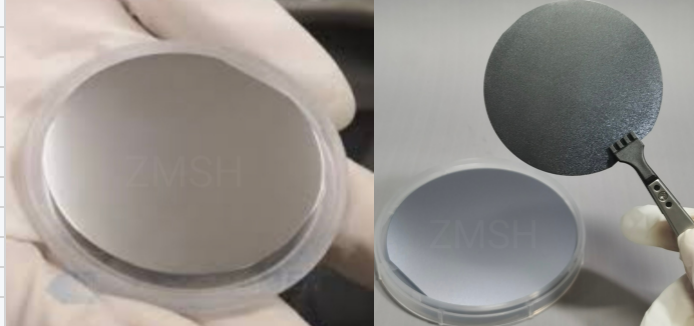
2’’ InSb-Te EPI Substrates Narrow Band Gap Semiconductor Substrates
Hall Components
Description of InSb-Te:
Indium antimonide (InSb), as a kind of group ⅲ-V binary compound semiconductor material,
has been the focus of research in the field of semiconductor materials since its discovery with stable physical and chemical
properties and excellent process compatibility. InSb has a very narrow band gap, a very small electron effective mass and a very high electron
mobility, especially noteworthy is that it belongs to the intrinsic
absorption in the spectral range of 3-5 μm, with nearly 100 percent quantum efficiency, making it the
preferred material for the preparation of medium-wave infrared detectors, and the application prospect and commercial demand are huge.The
lattice structure size of te atom and sb atom is close to each
other, and the valence electron shell structure is also close to
each other. te atom is doped as a substitute to replace sb in the
crystal and plays the role of donor. It was found that the CZ-pull method could be used to prepare insb body materials with a certain
te doping concentration, and the addition of te could change the
conductive type of insb crystals, and also had an important impact
on the electrical and optical properties of the materials. Relevant
studies laid the experimental foundation for the spatial growth of Te Doped InSb.
Features of InSb-Te:
| High carrier concentration | It has higher electrical conductivity and low resistivity in
electronic devices. |
| High carrier mobility | It describes the carriers in a material to move under an electric
field. |
| Determine the nature | Tellurium doping can increase the heat of InSb crystal materials‘
Stability. |
| Light absorption | Tellurium doping can change the band junctions of InSb crystals
Structure. |
| Light emission | Te-doped InSb can be stimulated to produce light emission by
external excitation or electron injection. |
| Compatibility | The TE-doped InSb substrate has good lattice matching with other
semiconductors. |
| Thermal stability | Tellurium doping can improve the thermal stability of InSb
materials. |
| Optical property | Tellurium doping also has a certain effect on
the optical properties of InSb materials |
Technical Parameters of InSb-Te:
Parameter | InSb-Te-2in-510um-PP |
Growth method | CZ |
Dopant | Te |
Orientation | (111)+/-0.5° |
Orientation angle | N/A |
Edge rounding | 0.25 |
Diameter | 50.5+/-0.5 |
Thickness | 510+/-25 |
OF orientaiton | EJ[01-1]+/-0.5° |
OF length | 16+/-2 |
IF orientation | EJ[01-1]+/-0.5° |
IF length | 8+/-1 |
CC | 0.4-1.4E5@77K |
Mobility | >100000@77K |
EPD-AVE | ≤50 |
TTV | ≤10 |
TIR | ≤10 |
BOW | ≤10 |
Warp | ≤15 |
Front Surface | Polished |
Back side surface | Polished |
Pachaging | Single tray |
Applicstions of InSb-Te:
1. High-speed electronic devices: tellurium-doped InSb crystals
also have potential in high-speed electronic devices.
2. Quantum structure devices: InSb crystals doped with Te can be
used to prepare quantum structure devices, such as
quantum Wells and quantum dot devices.
3. Optoelectronic devices: InSb crystals doped with Te can be used
to prepare various optoelectronic devices, such as
photodetectors, photoelectric amplifiers and photoelectric
converters.
4. Infrared detector: InSb crystals doped with Te can be used to
prepare high-performance infrared detectors. Because
tellurium doping can increase the carrier concentration and carrier
mobility.
5. Infrared lasers: InSb crystals doped with Te also have
application potential in the field of infrared lasers. By
introducing
tellurium doping into InSb crystals, the band structure of INSB
crystals can realize the work of infrared lasers.
Other Related Product to InSb-Te:
SIC
Substrate:

FAQ:
Q: What is the Brand Name of Te-InSb?
A: The Brand Name of Te-InSb is ZMSH.
Q: What is the Certification of Te-InSb?
A: The Certification of Te-InSb is ROHS.
Q: Where is the Place of Origin of Te-InSb?
A: The Place of Origin of Te-InSb is CHINA.
Q: What is the MOQ of Te-InSb at one time?
A: The MOQ of Te-InSb is 25pcs at one time.


