Sign In | Join Free | My himfr.com
Home > GaAs Wafer >

500um Thickness Indium Arsenide Wafer InAs Crystal Wafer 2 Inch Diameter 50.8mm

SHANGHAI FAMOUS TRADE CO.,LTD
Trust Seal
Verified Supplier
Credit Check
Supplier Assessment
Contact Now
    Buy cheap 500um Thickness Indium Arsenide Wafer InAs Crystal Wafer 2 Inch Diameter 50.8mm from wholesalers
     
    Buy cheap 500um Thickness Indium Arsenide Wafer InAs Crystal Wafer 2 Inch Diameter 50.8mm from wholesalers
    • Buy cheap 500um Thickness Indium Arsenide Wafer InAs Crystal Wafer 2 Inch Diameter 50.8mm from wholesalers
    • Buy cheap 500um Thickness Indium Arsenide Wafer InAs Crystal Wafer 2 Inch Diameter 50.8mm from wholesalers

    500um Thickness Indium Arsenide Wafer InAs Crystal Wafer 2 Inch Diameter 50.8mm

    Ask Lasest Price
    Brand Name : zmsh
    Model Number : InAs wafer
    Price : by case
    Supply Ability : 500pcs/month
    Delivery Time : 1-4weeks
    • Product Details
    • Company Profile

    500um Thickness Indium Arsenide Wafer InAs Crystal Wafer 2 Inch Diameter 50.8mm

    2inch diameter 50.8mm 500um thickness InAs substrates,Indium arsenide InAs crystal wafer, N-type 3inch 0.6mm InAs wafer,10x10mm square InAs wafers
    ------------------------------------------------------------------------------------------------------------------------------

    InAs single crystal substrate can be grown InAsSb/In - AsPSb InNAsSb heterostructure materials,such as making 2 ~ 14 microns of infrared wavelength light-emitting devices, with InAs single crystal substrate can also be grown epitaxial AlGaSb superlattice materials, production for infrared quantum cascade lasers.

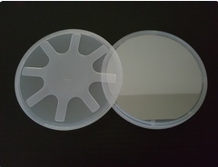
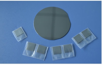
    ZMKJ can provides InAs wafer ( Indium Arsenide ) to optoelectronics industry in diameter up to 3 inch .

    InAs crystal is a compound formed by 6N pure In and As element and is grown by Liquid Encapsulated Czochralski ( LEC ) method with EPD < 15000 cm -3 . InAs crystal has high uniformity of electrical parameters and low defect density , suitable for MBE or MOCVD epitaxial growth . We have "epi ready " InAs products with wide choice in exact or off orientation , low or high doped concentration and surface finish . Please contact us for more product information .

    General Properties

    COMMON SPECIFICATIONS
    crystaldopetype
    carrier concentration
    cm-3
    mobility rate(cm2/V.s)
    dislocation density
    (cm-2)
    size
    InAs
    N
    5*1016
    2*104
    <5*104
    Φ2″×0.5mm
    Φ3″×0.6mm
    InAs
    Sn
    N
    (5-20)*1017
    >2000
    <5*104
    Φ2″×0.5mm
    Φ3″×0.6mm
    InAs
    Zn
    P
    (1-20) *1017
    100-300
    <5*104
    Φ2″×0.5mm
    Φ3″×0.6mm
    InAs
    S
    N
    (1-10)*1017
    >2000
    <5*104
    Φ2″×0.5mm
    Φ3″×0.6mm
    size(mm)
    Dia50.8x0.5mm,10×10×0.5mm,10×5×0.5mmalso can be customized
    RaSurface roughness(Ra):<=5A
    polished1sp or 2sp
    package
    100 grade packing in1000grade cleaning room

    GrowthLEC
    DiameterØ 2" / Ø 3"
    Thickness500 um ~ 625 um
    Orientation<100> / <111> / <110> or others
    Off orientationOff 2° to 10°
    SurfaceOne side polished or two sides polished
    Flat optionsEJ or SEMI. Std .
    TTV<= 10 um
    EPD<= 15000 cm-2
    GradeEpi polished grade / mechanical grade
    PackageSingle wafer container


    ABOUT OUR ZMKJ

    ZMKJ locates in the city of Shanghai, Which is the best city of China, and our factory is founded
    in Wuxi city in 2014.We specialize in processing a varity of materials into wafers, substrates
    and custiomized optical glass parts.components widely used in electronics, optics,
    optoelectronics and many other fields. We also have been working closely with many domestic
    and oversea universities, research institutions and companies, provide customized products
    and services for their R&D projects.
    It's our vision to maintaining a good relationship of cooperation with our all customers by our
    good reputatiaons. so we also can provide some other materials substrates as like:
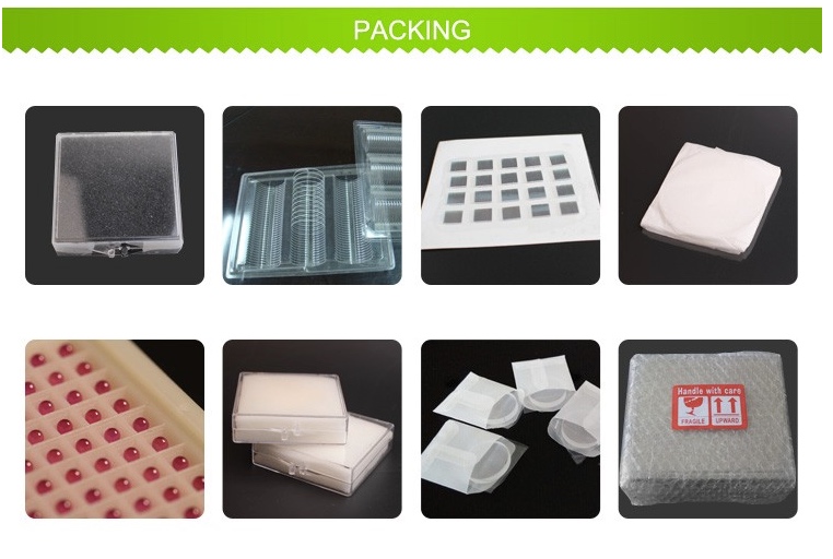
    Packaging – Logistcs
    Worldhawk concerns each details of the package , cleaning, anti-static , shock treatment .
    According to the quantity and shape of the product , we will take a different packaging process!
    FAQ –
    Q: What you can supply logistics and cost?
    (1) We accept DHL, Fedex, TNT, UPS, EMS, SF and by FOB
    and pay condition of 50% deposit,50% before delivery.
    Q: What's the delivery time?
    For inventory: the delivery is 5 workdays after order.
    For customized products: the delivery is 2 or 3 workweeks after order.

    Q: What's the MOQ?
    (1) For inventory, the MOQ is 5pcs.
    (2) For customized products, the MOQ is 10pcs-30pcs.
    Q: Do you have inspection report for material?
    We can supply detail report for our products.


    Product Tags:

    gaas wafer


    indium arsenide wafer

      
    Quality 500um Thickness Indium Arsenide Wafer InAs Crystal Wafer 2 Inch Diameter 50.8mm for sale
    Inquiry Cart 0
    Send your message to this supplier
     
    *From:
    *To: SHANGHAI FAMOUS TRADE CO.,LTD
    *Subject:
    *Message:
    Characters Remaining: (0/3000)